 We’ve all heard the phrase that timing is everything. Nowadays, the buses that connect, for example, processors to main memory require very precise timing, in the order of tenths of nanoseconds. Manufacturers provide all this information in their datasheets, but it needs to be combined with the appropriate Input/output Buffer Information Specification (IBIS) models and PCB (printed circuit board) construction characteristics, such as trace impedances, their length, number of loads and their distribution, etc.
Thus, all manufacturers test their devices to make sure they meet the specifications set out in the above-mentioned datasheets. These tests are performed under the same operating conditions specified in said documents, such as voltage ranges, test impedances, reference voltage, temperature ranges, etc. The tests in question are performed by mounting the device under test (DUT) on a tester, where, connected to a test card, the reference impedance specified in the datasheet is presented to each output pin. In addition, the tester can provide the DUT with the signal combination it needs to operate with the specified slew rate, the clock signals of the required frequency, and simultaneously measure (with extreme accuracy) the timing at the device pins.
However, when you consider that in a real circuit the trace load and topology will usually be different to the test ones, it begs the question as to whether we can really obtain any useful information from datasheets. The answer is yes, with the help of simulation tools, such as HyperLynx, using the IBIS models provided by the manufacturer. And that is precisely the intention of this blog post, though, for brevity’s sake, we will only present a simple example.
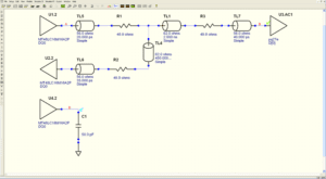
To illustrate, imagine the hypothetical case that we want to calculate – without needing to manufacture prototypes – the maximum operating frequency of the memory interface if the data bus has the same topology for all the bits as in the upper circuit in Fig. 2 – where a PowerQUICC II (U3) mounts 64 MB of main memory, in the form of two -7E 256 Mbit (U1 and U2) SDRAM[1] chips, for example.
The condition that would have to be met [2] would be:
tCK ≥ tAC + tp + t(sp13) (1)
Where:
tCK → Clock period whose value we want to obtain.
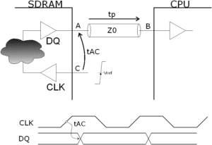
tAC → Time taken to access the data from the moment the rising clock edge crosses the Vref reference level at point C in Fig. 1, until the data reaches point A in the same figure.
tp → Data propagation time from point A to point B.
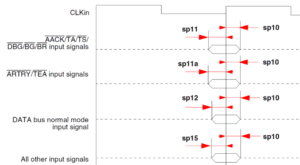
t(sp13) → Minimum time data must be stable at point B before the next clock edge so they are correctly sampled by the CPU (setup time).
The above inequality presents two problems, namely:
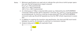
• Usually, the access time (tAC) cannot be obtained from the datasheet, since the load seen by U1.2 at point A in Fig. 2 differs from the 50 pF reference load seen by U4.2, which corresponds to the test assembly which the manufacturer uses to obtain tAC(CL) [3].
• A value can be obtained from the simulator that is “similar” but not exactly the same as (tAC + tp). This is because using tAC means taking the Vref crossing at point C in Fig. 1 as the time origin, while the time origin in the simulator is an unknown instant to which the driver output excitation is applied.
However, by slightly manipulating the inequality and after converting it into an equation, which is the condition that makes the minimum period, we can rewrite (1) as follows:
tCKmin = tAC(2) + [ (tAC + tp) – tAC(2) ] + t(sp13) (2)
Now the expression in square brackets, referred to in the literature as compensation time, or Tcomp, is independent of the time origin and can be obtained by means of simulation.
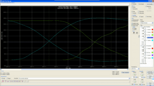
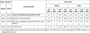
The extracts included in Table 1 and Table 2 give us the values tAC(2) = 5.4 ns and t(sp13) = 1.5 ns. And from the simulation, we get the difference [ (tAC + tp) – tAC(2) ] which, as stated above, is independent of the time origin. Thus, since both the green (DQ0 in B) and blue (DQ0 in D) traces in Fig. 3 share the origin, we can directly subtract their values to get 2.59 ns (= 5.2895 ns[4] – 2.7078 ns). By inserting the above values into equation 2 we get:
tCKmin = 5.4 ns + 2.59 ns + 1.5 ns = 9.49 ns ⇒ fmax = 105 MHz
In Teldat devices, it is often necessary to evaluate the viability and potential of particular topologies before manufacturing prototypes. Simulation tools not only allow calculations such as those shown above, they also allow you to preview a signal’s waveform as if on an oscilloscope screen, calculate terminations to minimize reflections, avoid signal integrity problems or crosstalk (thus reducing unwanted electromagnetic emissions) and, ultimately, avoid costly (time and money) design iterations.
Figure 1
[1] SDRAM was chosen over newer RAMs like DDR4 or 5 because the levels are LVTTL which are more familiar.
[2] Equation (1) assumes that the clock signal is distributed in such a way that when it crosses through Vref in memory (point C in Fig. 1) it also crosses through Vref in the processor (this point is not shown in the figures), i.e., there is no skew between the two clocks.
[3] tAC(CL) is the time measured in the tester from the moment the rising clock edge crosses the reference level at point C in Fig. 1, until the data reaches that same level on the C1 capacitor that charges U4 in Fig. 2 (point D).
[4] This value corresponds to the DQ0 high to low level transition through VIL (0.8 volts). An explanation of this is of little interest for the purpose of this entry.

